Test Engineering. Failure Analysis. Answers.
|
|
Search



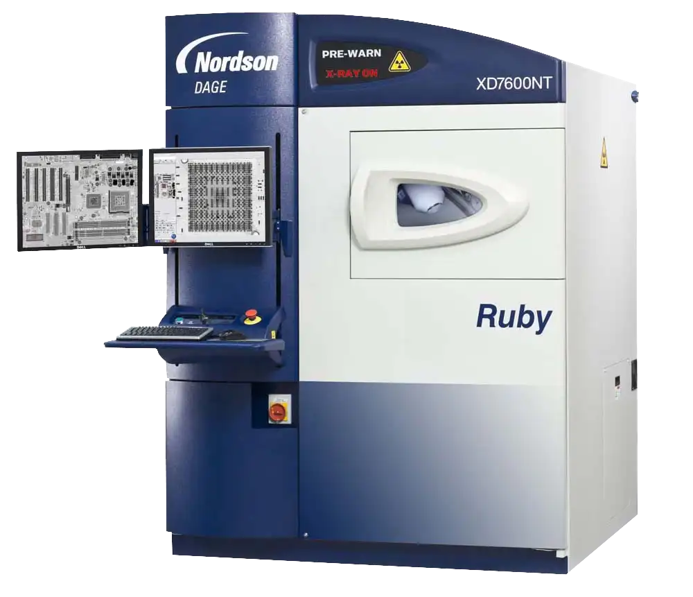
Nordson Dage XD7600NT500 Ruby
Somewhere in There, the Signal Stops
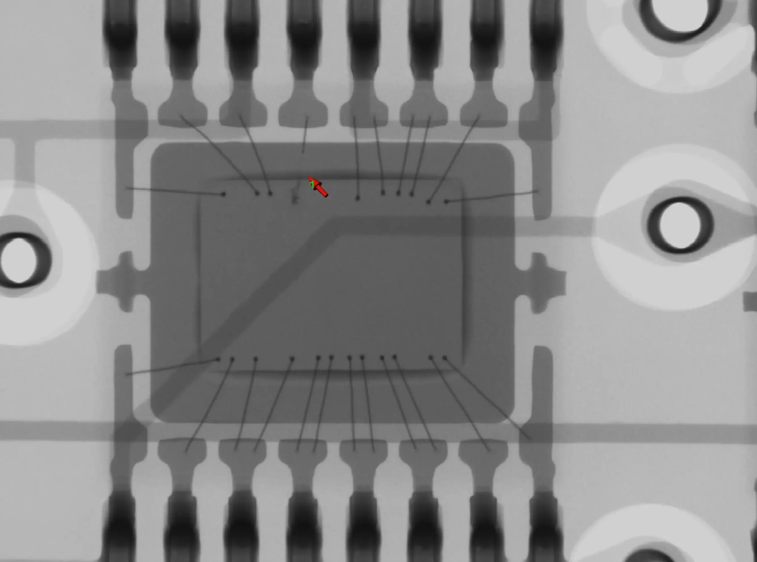
When the Connection Fails
Microscopic failures can bring an entire assembly down.
2D and oblique X-ray inspection make it possible to evaluate internal wire bonds, die attach conditions, and package integrity without destroying the component.
Perfect for:
• Broken or lifted bond wires
• Semiconductor package analysis
• Microelectronic failures
• Burned or damaged devices
• Process verification
• Root cause investigations
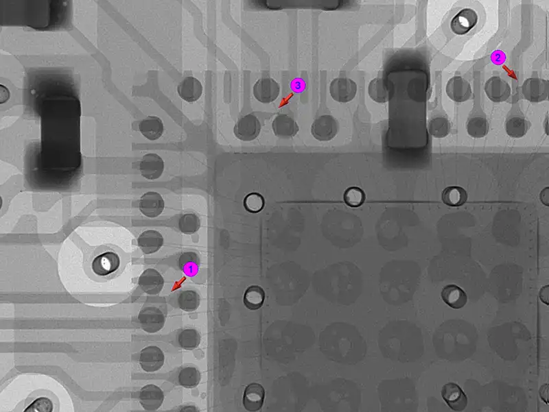
Finding the Break Nobody Can See
Sometimes the problem is hiding inside the board.
Using high-resolution 2D and oblique X-ray imaging, we can locate open circuits, broken traces, internal defects, and hidden manufacturing issues that traditional inspection methods miss.
Perfect for:
• Broken internal traces
• Open circuits and intermittent failures
• PCB defect analysis
• Hidden solder joint evaluation
• Manufacturing defect verification
• Failure analysis and troubleshooting
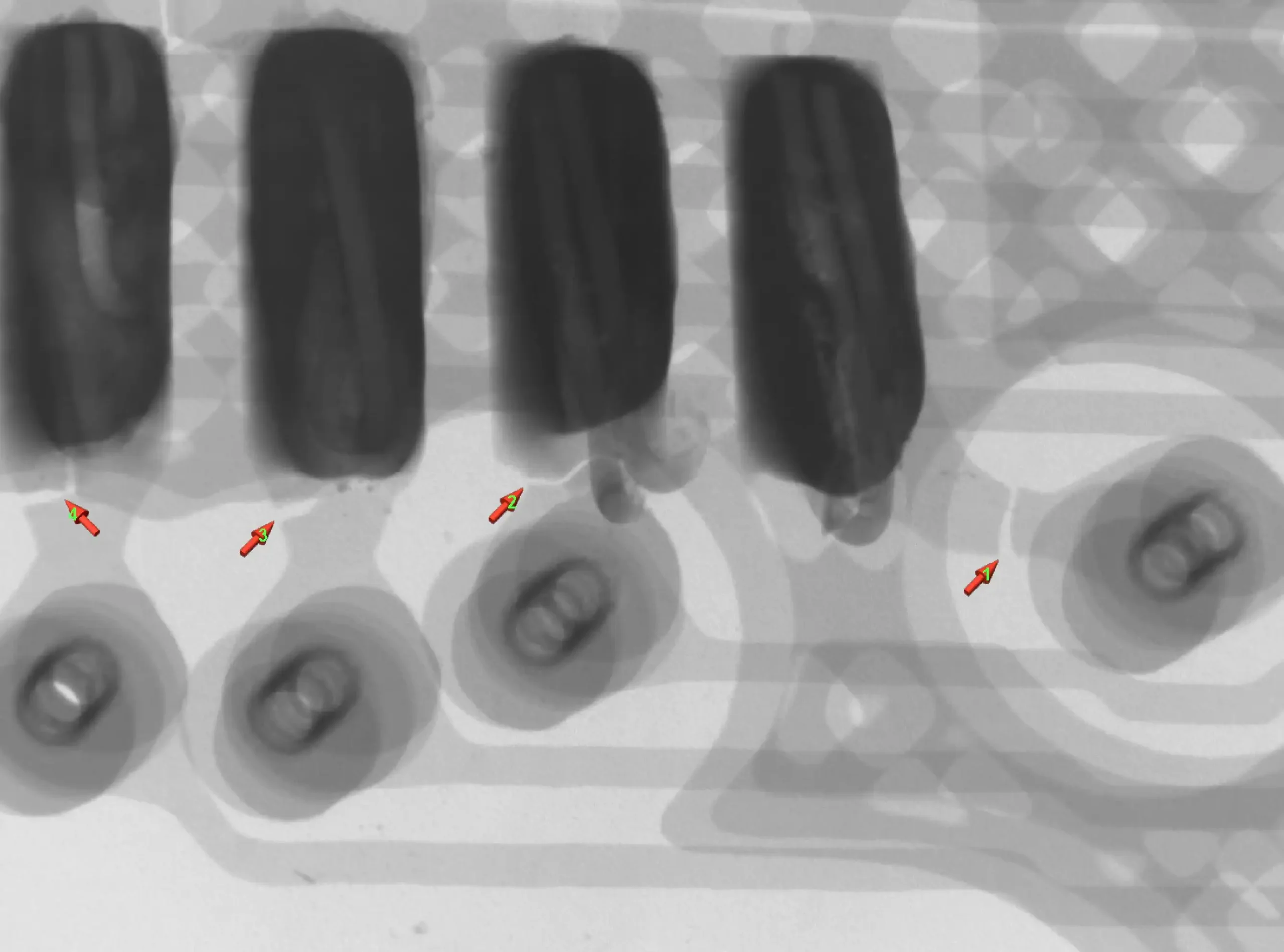
When Separate Connections Become One
Sometimes the defect is exactly what it looks like.
Standard 2D imaging quickly identifies solder bridges, shorts, and other manufacturing defects that impact electrical performance.
Looking Beyond the Surface
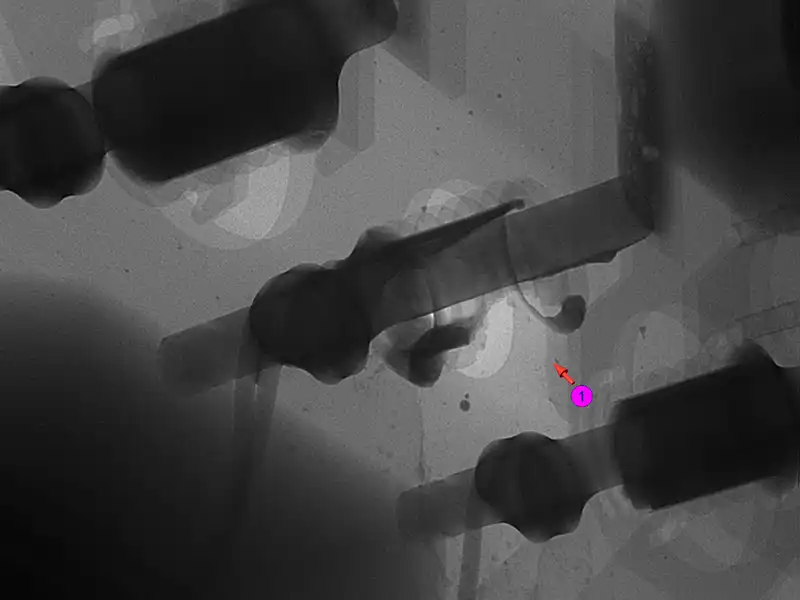
Sometimes the answer requires a different angle.
By adjusting the viewing perspective, we can evaluate plated through-holes, hidden joints, and internal damage that may not be obvious from a single view.
What We Inspect
If it’s safe to X-ray and fits in our system… we’ll take a look.
Let’s See What’s Going On Inside
Have a part that’s confusing everyone?
Need help on a contract that requires CT?
Trying to figure out if 2D or 3D is right for you?